• GPU Knowledge Hub
  • Repair Warranty Claim
  • Shop
Book Repair My Account
GPU Solutions

[email protected]
Email Us

GPU Solutions
Back To Gaming

Navigation
  • Home
  • Services
  • FAQ
  • Book Repair
  • Repair Enquiry
  • Sell GPU
  • Contact Us
  • About
Your Cart Details

Cart

RTX 3070 8GB to 16GB VRAM Upgrade – Complete Guide with Real-World Cases

Hi, my name is Frazer and welcome to GPU Solutions. Over the last few months, I’ve worked on several RTX 3070 8GB → 16GB upgrades across different brands and conditions:

  • A ZOTAC RTX 3070 proof-of-concept upgrade that initially had a black screen after load.
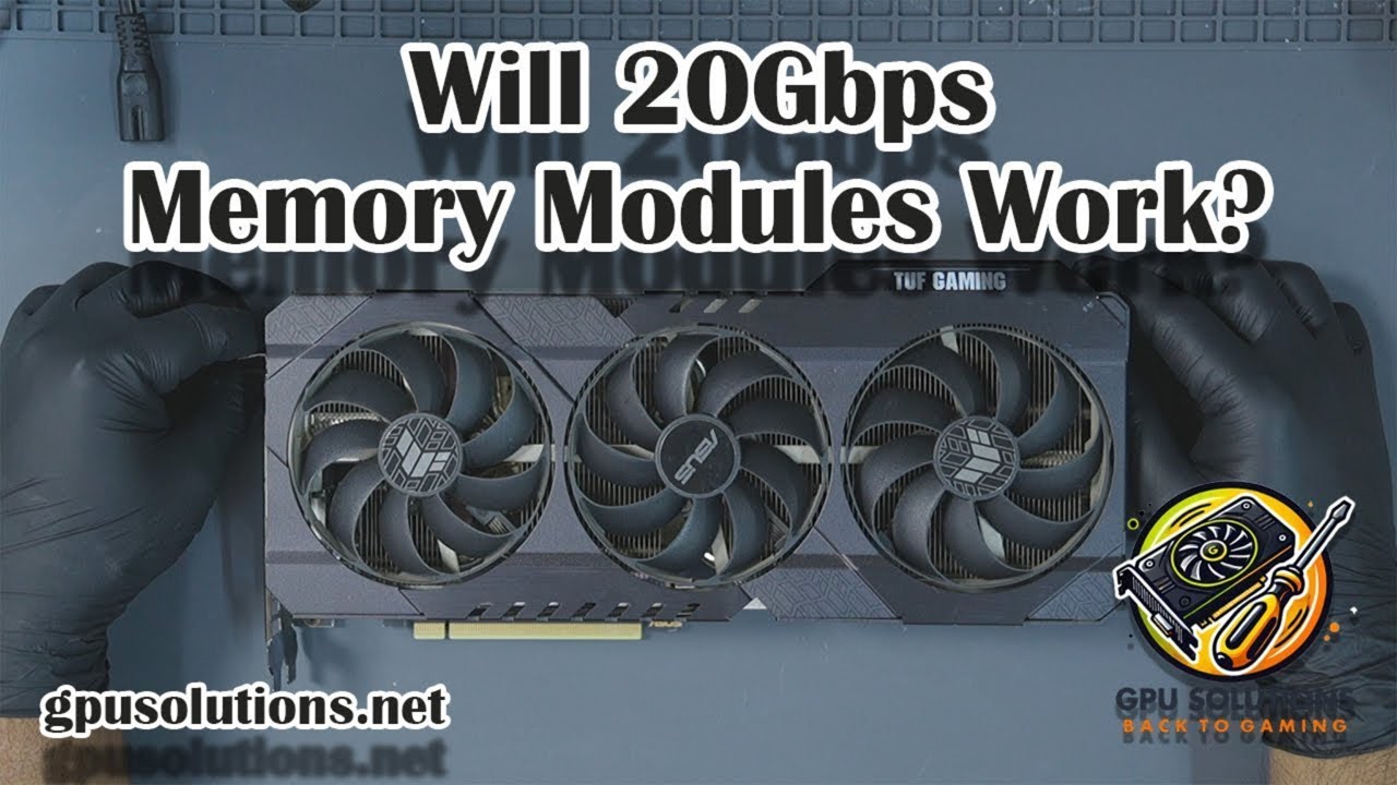
  • An ASUS TUF RTX 3070 where the customer requested 20Gbps memory modules – and we found out why that doesn’t work.
  • An ASUS Noctua RTX 3070 that arrived after a failed DIY attempt, with exposed traces and missing components, and was fully repaired and upgraded.

This article combines all three stories into one detailed guide so you can understand:

  • Why upgrading an RTX 3070 to 16GB can matter.
  • What is technically happening under the hood (VRAM, straps, BIOS limits).
  • What can go wrong – and how I fixed it in each case.

Important: this is not a beginners’ how-to. These are advanced, high-risk modifications that require solid BGA rework skills and proper tools. Attempt them at your own risk.


Why 8GB on RTX 3070 Is Becoming a Problem

On paper, the RTX 3070 is a powerful card. But its 8GB VRAM is increasingly a bottleneck in modern games.

In demanding titles like Cyberpunk 2077, The Last of Us Part I, or Microsoft Flight Simulator, it’s easy to push past the 8GB VRAM limit, especially at 1440p and 4K with high or ultra textures.

When that happens, this is what you typically see:

  • Stuttering and frame-time spikes
  • Lag when you pan the camera or move into new areas
  • Occasional crashes or black screens in extreme cases

Why? Because once VRAM is full, the GPU starts spilling into system RAM, which is much slower. Latency goes up, frame pacing falls apart, and your experience suffers—even if your FPS counter looks okay.

Upgrading from 8GB to 16GB doesn’t magically increase raw GPU compute, but it gives the card a much larger buffer to hold high-resolution textures and game data, which can:

  • Improve 1% and 0.1% lows
  • Reduce stutter when VRAM-heavy scenes load
  • Help “future-proof” the card for upcoming games that expect more than 8GB

How the RTX 3070 8GB → 16GB Upgrade Works

An RTX 3070 16GB mod relies on a few key facts:

  1. It uses GDDR6 memory, not GDDR6X.
  2. The stock card uses 1GB Samsung GDDR6 chips.
  3. You can swap those for 2GB Samsung GDDR6 chips of the same generation (14Gbps or 16Gbps).
  4. The PCB and BIOS support the correct memory configuration when the strap resistors are set properly.

In simple terms:

  • You remove all 1GB GDDR6 memory chips.
  • You install 2GB GDDR6 chips in the same positions.
  • You reconfigure the strap resistors so the BIOS knows it now has 2GB Samsung modules per channel.
  • The card then exposes 16GB VRAM to the driver and operating system.

Straps in short: strap resistors are tiny 100kΩ resistors that sit on specific lines. If a strap is tied to 1.8V, it represents a binary 1. If it’s tied to ground, it represents a 0. The combination (for example, 1-1-0) tells the BIOS which memory type/capacity is installed.


Case 1 – ZOTAC RTX 3070: First 8GB → 16GB Mod & the Black Screen Issue

Step 1 – Memory Swap

The first RTX 3070 I upgraded was a ZOTAC RTX 3070. It arrived with:

  • Samsung 1GB GDDR6 modules (8 chips = 8GB total).
  • Fully working core and VRM.

The plan was to replace those with 2GB Samsung GDDR6 modules. In the first round I used 2GB 14Gbps Samsung chips, later I also tried 2GB 16Gbps variants when troubleshooting.

The process:

  • Preheat the board on a preheater.
  • Use hot air to remove all original memory modules.
  • Clean the pads with flux, solder wick and isopropyl alcohol until they’re flat and shiny.
  • Install new 2GB Samsung GDDR6 modules using hot air reflow.

Once everything cooled down, I ran MATS (NVIDIA’s memory test) to verify the installation. MATS passed, which confirmed that the memory was soldered and connected correctly.

Step 2 – Setting the Straps for 2GB Samsung

Next, I needed the BIOS to correctly recognize the 2GB Samsung modules. That’s where strap resistors come in.

On this ZOTAC board, the strap network uses three strap bits that can be set to either high (1.8V) or low (ground). For 2GB Samsung, the correct combination was:

  • Strap 2: 1 (high)
  • Strap 1: 1 (high)
  • Strap 0: 0 (low)

In short: 1-1-0.

I located the strap resistors, moved the 100kΩ parts into the appropriate positions (high or low), cleaned up, reassembled the card, and installed it on the test bench.

In Windows, GPU-Z reported 16GB of VRAM and MATS still passed. So at this stage, the mod was technically working.

Step 3 – The Strange Black Screen After Load

Under stress, the GPU behaved well:

  • FurMark – ran fine under full load.
  • Superposition – passed.
  • Heaven – passed.
  • OCCT – I pushed memory utilization to over 14GB and it still passed.

But there was one big problem: as soon as the load stopped, the system would go to a black screen. No signal. The card would crash when coming off load.

I suspected:

  • Power delivery to the memory (30A FETs on the memory rail).
  • Combined with PSU voltage drop (12V sagging to around 11V under load).

I tried:

  • Reballing the GPU core.
  • Changing from 14Gbps to 16Gbps 2GB modules.

The behavior stayed the same: stable under load, black screen when the stress test stopped.

Step 4 – The Fix: Nvidia Control Panel Power Management

Several viewers suggested trying a power management tweak in the Nvidia Control Panel. The key setting is:

  • 3D Settings → Power management mode → Prefer maximum performance

Once I changed that, the behavior completely changed:

  • Stress tests ran fine.
  • Stopping tests no longer caused black screens.
  • The card stayed stable on the desktop and in normal use.

This workaround keeps the GPU from aggressively power-saving between load and idle, which seems to be what was causing the instability on this specific mod.

Step 5 – Real-World Gaming Tests

To verify that the upgrade and fix were truly practical, I moved the card to my Ryzen 9 5950X workstation and tested:

  • Red Dead Redemption 2
  • Far Cry 6 (benchmark, 1440p, ultra, FSR off)
  • A Plague Tale: Requiem (ultra settings with ray tracing)

In these tests:

  • VRAM usage could exceed 8GB, sometimes reaching up towards 10GB+.
  • Gameplay remained smooth with no post-load black screens.
  • The system recognized and used the extra VRAM without issues.

Not all games will necessarily behave perfectly (NVIDIA doesn’t officially support 16GB on a 3070), but in these real tests the upgrade was fully usable.


Case 2 – ASUS TUF RTX 3070: Why 20Gbps Memory Failed

Customer Request: 20Gbps 2GB Modules

Next, I worked on an ASUS TUF RTX 3070 sent in specifically for a 16GB upgrade. The customer had a special request: he wanted 2GB 20Gbps GDDR6 modules installed.

I hadn’t tried this combination before, so I treated it as an experiment to see if the BIOS would handle it.

Baseline Testing

Before any upgrade, I always check stability:

  • Install the GPU on the bench, boot to Windows, install drivers.
  • Run FurMark – core at around 65°C, hotspot around 77°C.
  • Run benchmarks:
    • Superposition: ~11,380
    • 3DMark Nomad: ~3,198
    • 3DMark Speedway: ~3,533

The GPU was stable and healthy, so it was safe to proceed.

Thermal Putty Problem

When I opened the card, I found thermal putty stuffed all around the core and memory modules.

That’s a serious problem:

  • Putty can creep under BGA chips over time.
  • It can lift pads, crack solder joints and cause “gray pad” failures.
  • On tightly packed GPUs (3080, 3090, 4090) it can force you to lift the entire core just to fix memory issues.

In this case, the 3070 layout is a bit more forgiving, but I still:

  • Removed all the putty around core and memory.
  • Cleaned thoroughly with isopropyl alcohol.

Attempt #1 – 2GB 20Gbps Modules

I removed all original memory, prepared the pads, and installed 2GB 20Gbps GDDR6 modules.

After installation:

  • MATS passed – the memory was soldered correctly.
  • I set the straps to the correct 16GB Samsung configuration:
    • On ASUS boards near the crystal: strap 2, strap 0, strap 1 (top to bottom).
    • For 2GB Samsung: strap 2 = high, strap 1 = high, strap 0 = low → 1-1-0.

However, when I booted into Windows:

  • It showed the Windows logo.
  • Then either crashed or went to a black screen.

After multiple attempts, it was clear: the GPU would not boot properly with 20Gbps modules, even though MATS passed.

The conclusion: the BIOS had timings only for 14Gbps memory. It did not have valid entries for 20Gbps GDDR6, so the card simply couldn’t operate stably with those chips.

Attempt #2 – 2GB 16Gbps Modules (Success)

I contacted the customer, explained the situation, and he agreed to switch to 2GB 16Gbps Samsung GDDR6 modules instead.

The procedure was identical:

  • Remove the 20Gbps modules.
  • Prepare the pads again.
  • Install the 2GB 16Gbps modules.
  • Set the same 1-1-0 strap configuration.
  • Clean, reassemble, and test.

This time:

  • MATS passed.
  • Windows booted normally.
  • Drivers installed correctly.
  • GPU-Z reported 16GB of VRAM.

For extra stability, I again set Nvidia Control Panel → Power management mode → Prefer maximum performance.

Benchmarks After the Upgrade

With 16Gbps 2GB modules installed:

  • FurMark: core at ~62°C, hotspot at ~72°C (slightly better thermals after cleaning and fresh pads/paste).
  • Superposition: ~11,289.
  • 3DMark Nomad: ~3,162.
  • 3DMark Speedway: ~3,425.

The scores were slightly lower than the original baseline because the BIOS still runs the VRAM at 14Gbps timings. It doesn’t “know” we installed 16Gbps chips.

However, on these ASUS boards, 16Gbps modules can typically be safely overclocked by ~1000–1500MHz using MSI Afterburner (or another OC tool), which can recover or exceed the original performance.

Finally, I ran OCCT for 10 minutes, using the full memory pool. No errors, no instability. The card was ready to return to the customer as a working RTX 3070 16GB.


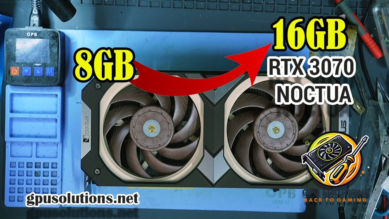
Case 3 – ASUS Noctua RTX 3070: Fixing a DIY Upgrade Gone Wrong

What the Card Looked Like on Arrival

The third card was an ASUS Noctua RTX 3070 – a huge, four-slot cooler – and it arrived after a failed DIY VRAM upgrade attempt.

The owner had:

  • Already removed the original memory chips.
  • Sent the card to me along with new memory modules from AliExpress.

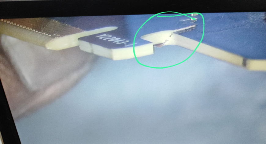
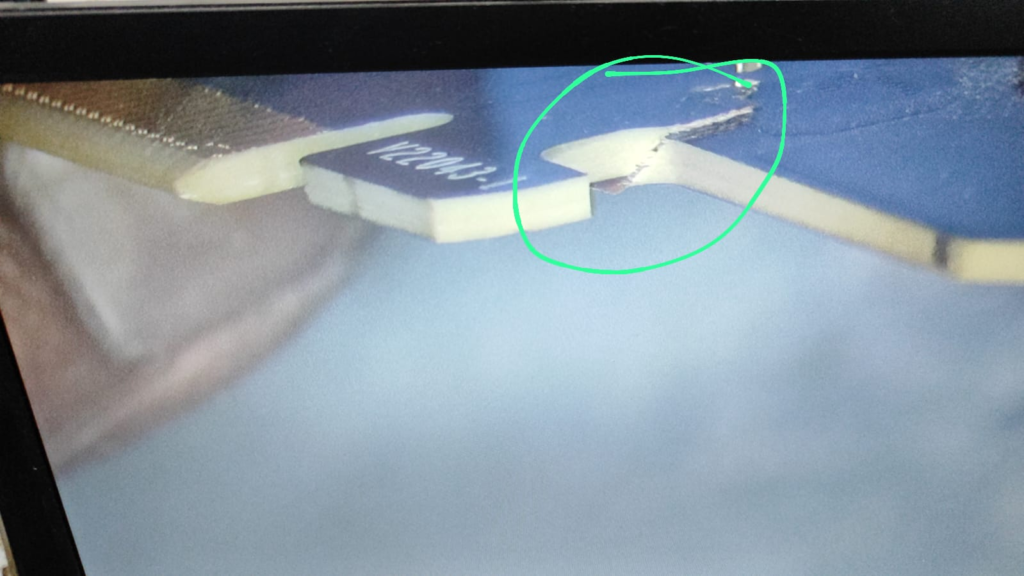
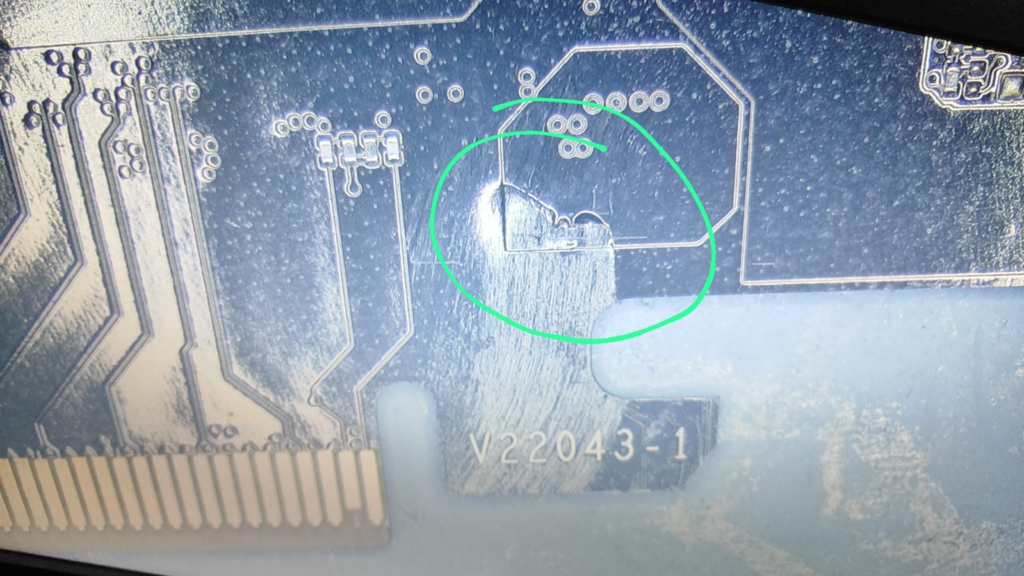
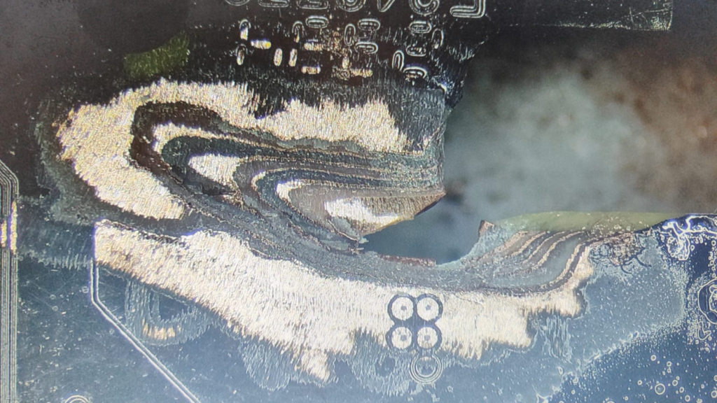
Under the microscope, I saw:

  • Pads that weren’t flat and had a gray appearance (usually too much heat or too little flux).
  • Scraped solder mask exposing copper traces.
  • Some knocked-off components (capacitors and resistors).

To be fair, the memory removal wasn’t the worst I’ve seen, but leaving exposed copper and missing components is a serious problem for reliability.

Step 1 – Repairing the PCB

I started by:

  • Preheating the board to around 120°C.
  • Adding leaded solder to the pads to reduce the melting point.
  • Using solder wick to flatten the pads properly.
  • Cleaning everything with 99.9% isopropyl alcohol.

Then I addressed the damage:

  • Applied UV solder mask to cover exposed copper traces.
  • Cured the mask.
  • Replaced missing components (filter capacitors and critical resistors) from a donor board.

Once all components were replaced and the pads were in good condition, I double-checked resistance to confirm there were no shorts and that the rails looked normal.

Step 2 – Installing New Memory Modules

With the board repaired, I:

  • Preheated the PCB again.
  • Applied flux to both the PCB pads and the new memory modules.
  • Aligned each chip and used hot air to reflow them into place.

Alignment doesn’t need to be microscopically perfect; as long as you’re close, surface tension during reflow will pull the chip into the correct position. But you must avoid overheating and pad damage.

After installing all modules and letting the board cool, I ran MATS. It passed, confirming that all memory chips were correctly soldered and making proper contact.

Step 3 – Setting the Straps

Just like the other boards, this Noctua uses three strap bits near the crystal:

  • Top: strap 2
  • Middle: strap 0
  • Bottom: strap 1

Originally, with 1GB Samsung modules, the configuration was 0-0-0 (all low). For 2GB Samsung, the correct configuration is 1-1-0:

  • Strap 2 = high
  • Strap 1 = high
  • Strap 0 = low

I moved the 100kΩ resistors accordingly, cleaned the area, and reassembled the card.

Step 4 – Pads, Paste & Final Testing

Since this card arrived without proper thermal pads, I installed new 2mm pads on both memory and MOSFET areas, applied fresh thermal paste to the GPU core, and put the cooler back on.

On the test bench:

  • Windows installed the drivers correctly.
  • GPU-Z reported 16GB of VRAM.
  • The Nvidia control panel was set to Prefer maximum performance.

I then ran:

  • FurMark – temps normal, no instability.
  • Superposition 4K Optimized – score around 11,269.
  • 3DMark Nomad and Speedway – healthy scores, no crashes.

The repair and the upgrade were both successful. This ASUS Noctua RTX 3070 went from a damaged, non-booting DIY attempt to a fully working 16GB card.


Tools & Skill Level Required

If you’re even thinking about attempting a 3070 VRAM upgrade yourself, here’s what you realistically need:

  • Microscope – for inspecting pads, traces and solder joints.
  • Preheater – to gently and evenly warm the board from below.
  • High-quality flux – to ensure proper wettability and prevent oxidation.
  • Hot air / BGA rework station – for safe removal and installation of memory chips.
  • Soldering iron – for pads cleanup and small component work.
  • Solder wick – to flatten pads and remove excess solder.
  • Leaded solder wire – to mix with lead-free solder and reduce the melting point.
  • Correct 2GB GDDR6 memory modules – from a reliable source.
  • 99.9% isopropyl alcohol – for cleaning.
  • Boardview and schematics (where available) – to identify straps and key components.
  • Test bench – for initial power-on and diagnostics.
  • Memory testing software (MATS/MODS, OCCT, etc.) – to verify VRAM integrity.
  • Stress testing tools – FurMark, Superposition, 3DMark, etc., to validate stability.

On top of that, you need experience. I strongly recommend learning on dead boards first. Removing and reinstalling BGA memory without lifting pads or damaging traces takes time and practice.


When an RTX 3070 16GB Upgrade Makes Sense

An RTX 3070 16GB mod is most relevant if:

  • You already own a good RTX 3070 and want to extend its life.
  • You play VRAM-heavy games at 1440p or 4K with high/ultra textures.
  • You do workloads (light AI, content creation) where extra VRAM can help.
  • You’re okay with the fact that this is unsupported by NVIDIA and some games may behave oddly.

It’s less about raw FPS gains and more about smoother performance under heavy VRAM use and giving an already capable GPU more headroom for modern and future titles.


Final Thoughts

Across three different RTX 3070s – a ZOTAC, an ASUS TUF and an ASUS Noctua – the story is consistent:

  • 2GB GDDR6 Samsung modules + correct strap configuration + good BGA work = a working 16GB RTX 3070.
  • 20Gbps modules don’t work when the BIOS only has timings for 14Gbps – even if MATS passes.
  • Driver and power management quirks can matter; the “Prefer maximum performance” tweak in the Nvidia control panel was key to solving the black screen issue on the first mod.
  • DIY attempts without proper tools and experience can cause significant damage, but they can sometimes be repaired if no critical pads are torn.

If you enjoyed this deep dive into GPU upgrades and repairs, you can:

  • Watch the full upgrade videos on my YouTube channel GPU Solutions.
  • Like, comment and share if you found it helpful.
  • Support the channel via memberships or the Thanks button – this helps fund more experiments like these.

Thanks for reading, and I’ll see you in the next repair or upgrade story. Cheers!

Book Your Upgrade. Select the brand, select RTX 3070, fill in your information, and submit.

YouTube player
YouTube player
YouTube player
YouTube player

Can Any GPU Be Upgraded? Understanding VRAM Limits with Real Examples

Hi, my name is Frazer and welcome to GPU Solutions. If you’re new here, I take you inside the world of graphics card repairs, upgrades, and crazy mods that very few people would dare try.

In this article, I’ll walk you through the upgrade of an Asus RTX 2080 Ti from 11GB to 22GB – and more importantly, I’ll answer the most common questions that came in after my first 22GB upgrade video.

While the repair itself is happening in the background, we’ll talk about:

  • Whether any GPU can be upgraded to more VRAM
  • How memory compatibility and density limits really work
  • Which GPUs are good candidates for upgrades – and which aren’t
  • What extra VRAM actually does for gaming and AI
  • The real cost of a VRAM upgrade
  • Whether this is something you should try yourself

Can Any GPU Be Upgraded to Have More VRAM?

The short answer is no. Not every graphics card can be upgraded.

Whether a GPU can realistically be upgraded depends mainly on three things:

  1. The maximum supported memory density the GPU core and PCB were designed for.
  2. Whether the card’s BIOS has timings for higher-capacity memory modules.
  3. Whether the memory type and pinout are compatible (GDDR6 vs GDDR6X vs GDDR7, etc.).

Let’s break each of these down.

1. Memory Controllers, Layout and Clamshell Design

When a GPU core is designed, it has a fixed number of memory controllers. Each controller talks to one (or sometimes two) memory modules.

In some GPUs, manufacturers use a technique called clamshell – one memory chip on the front of the PCB and one directly behind it on the back. This effectively doubles the capacity per channel.

Examples of clamshell designs include:

  • RTX 3090
  • RTX 4060 Ti 16GB
  • RTX 9060 XT 16GB

If your GPU doesn’t have memory pads or slots on the back of the PCB, then clamshell isn’t an option. You’re limited to whatever is on the front side only.

2. BIOS Support and Memory Timings

When a GPU is built, the BIOS is written with all the parameters the card will run with:

  • Memory timings
  • Power limits
  • Fan curves
  • Voltage and frequency tables

For VRAM upgrades, the critical part is the memory timings table.

There are three major manufacturers producing modern GDDR memory:

  • Samsung
  • Micron
  • Hynix (often written as “Hynix” or “Highex” in older docs)

They produce different memory types:

  • GDDR5 (legacy)
  • GDDR5X (legacy)
  • GDDR6
  • GDDR6X
  • GDDR7

Micron is the only manufacturer for GDDR5X and GDDR6X. GDDR5 and GDDR5X for new GPU designs are effectively no longer produced.

Let’s look at two examples:

Example: RTX 4090 (GDDR6X)

  • Uses Micron GDDR6X memory.
  • Each memory module is 2GB.
  • The BIOS only has timings for Micron GDDR6X, at different speeds.
  • There are no timings for Samsung or Hynix, because they don’t produce GDDR6X.

Example: RTX 3070 (GDDR6)

  • Uses GDDR6 memory.
  • The BIOS usually contains timings for Samsung, Micron and Hynix.
  • Modules may exist at 14Gbps, 16Gbps, 20Gbps, and sometimes lower speeds like 12Gbps.

Depending on what memory NVIDIA or AIB partners tested during development, the BIOS may or may not contain timings for certain densities and speeds. For upgrades, we care about whether timings exist for higher-capacity modules (e.g., 2GB vs 1GB), not just different speeds.

3. Maximum Memory Density: How Far Can You Go?

Every memory generation has a practical maximum module capacity that has been produced:

  • GDDR6 / GDDR6X: up to 2GB per chip
  • GDDR7: currently up to 3GB per chip

That leads to some interesting theoretical possibilities:

  • A GPU using 1GB GDDR6 / GDDR6X modules could be doubled to 2GB per module (if the BIOS supports it).
  • A GPU using 2GB GDDR7 modules could theoretically be upgraded to 3GB per module (still untested territory).

Concrete examples:

  • RTX 2080 Ti – Uses 1GB GDDR6 modules for a total of 11GB. With 2GB modules, you can reach 22GB (which is exactly what this upgrade does).
  • Hypothetical RTX 5090 32GB – If it uses 2GB GDDR7 modules, in theory it could reach 48GB using 3GB chips. As of now, this remains untested.

Why You Can’t Mix GDDR6, GDDR6X and GDDR7

Even though some of these memory types share the same pin count, they are not interchangeable.

GDDR6 vs GDDR6X

  • GDDR6 and GDDR6X may have the same number of pins, but the data lines and command lines are not in the same positions.
  • GDDR6X is produced only by Micron and the PCB layout is tailored to that.

So you cannot:

  • Put a GDDR6 chip on a PCB designed for GDDR6X, or
  • Put a GDDR6X chip on a GDDR6 PCB.

GDDR7 vs Previous Generations

  • GDDR7 has more pins than GDDR6/GDDR6X.
  • The data and command lines are in different locations again.

That means:

  • GDDR7 cannot be used on GDDR6 / 6X PCBs.
  • GDDR6 / 6X cannot be used on GDDR7 PCBs.

Which GPUs Can’t Be Upgraded Further?

Any GPU that’s already using the maximum produced memory capacity for its generation cannot be upgraded further on the same PCB.

For example:

  • GPUs using 2GB GDDR6 / GDDR6X modules – Already at the density limit. No 4GB GDDR6/GDDR6X modules exist.
  • Many RTX 40-series GPUs – Already using 2GB GDDR6X on a fully populated bus. No upgrade path on the same PCB.
  • AMD RX 6000 / 7000 / 9000 series – Use 2GB GDDR6 modules with all memory slots populated. There’s simply no “bigger” chip to swap to.

Good Candidates for VRAM Upgrades

Some cards are excellent candidates because they tick all the boxes:

  • They use 1GB GDDR6 modules.
  • The PCB layout supports the full bus width.
  • The BIOS contains timings for 2GB modules.

Examples include:

  • RTX 2080 Ti 11GB → 22GB (as in this article)
  • RTX 3070 8GB → 16GB (also a strong candidate with the right layout)

On the other hand, cards like:

  • AMD RX 6000 / 7000 / 9000 series – Already use 2GB GDDR6, no further upgrade path.
  • RTX 40-series – Already on 2GB GDDR6X, again maxed out.

These simply don’t have a meaningful upgrade path on the original PCB.

What About RTX 4090 with 48GB?

Some of you have seen RTX 4090 cards with 48GB of VRAM and asked how that’s possible.

Those are not standard consumer cards:

  • They use a custom PCB with a clamshell layout.
  • They run on a custom BIOS and often custom drivers.
  • They are typically built for enterprise or specific workloads, not gaming.

This is very different from taking a consumer 4090 and simply swapping VRAM on the stock PCB.

Does More VRAM Increase GPU Performance?

The most common follow-up question: “Does more VRAM make the GPU faster?”

The short answer: It depends.

Gaming

Increasing VRAM capacity does not directly increase raw compute performance. The GPU core is still the same. What more VRAM does give you is:

  • Room for higher-resolution textures
  • Better 1% lows when the game is VRAM-hungry
  • Less stuttering when you’re close to VRAM limits

When a game runs out of VRAM (very common on 8GB cards now), it spills over into system RAM. System RAM is much slower than VRAM, which causes:

  • Stuttering
  • Frame-time spikes
  • Drops in FPS due to added latency

Many newer titles already exceed 8GB of VRAM, and in the future this is only going to become more common – sometimes even at 1080p depending on the game and settings.

So from a gaming standpoint:

  • Upgrading an 8GB card to 16GB is often more impactful than upgrading an 11GB card to 22GB.
  • The 2080 Ti 11GB → 22GB upgrade is more of a specialized / enthusiast mod than a universal gaming necessity.

AI and Compute Workloads

When it comes to AI, no amount of VRAM ever feels like enough.

AI workloads scale with:

  • Model size
  • Batch size
  • Sequence length / resolution, etc.

Even an RTX 6000 with 96GB can feel small depending on what you’re running. From a cost perspective:

  • RTX 4090 24GB – very powerful, but also expensive.
  • RTX 3090 24GB – cheaper than a 4090, still strong for many AI tasks.
  • RTX 2080 Ti 22GB – much cheaper than both as a high-VRAM budget option once upgraded.

So for someone on a budget, a 22GB 2080 Ti can hit a nice sweet spot for some workloads, even though it’s not the newest architecture.

How Much Does a VRAM Upgrade Cost?

If you’re sourcing memory yourself, the cost of GDDR6 memory (14Gbps / 16Gbps) typically works out to:

  • About $12–$16 per module (approximate range, depends heavily on supplier and region)

If you buy new (which I highly recommend), final cost will depend on:

  • Where you live
  • Shipping cost and import duties

On top of that, you should add around $100 as a service fee for the actual upgrade work if you’re paying a technician.

For customers sending GPUs to me, the pricing (including memory) is approximately:

  • RTX 3070 upgrade: around $205
  • RTX 2080 Ti upgrade: around $235

So it only makes sense if your goal is to extend the useful life of a GPU you already own, or to enable a specific workflow that needs the extra VRAM.

Is This Something You Should Try Yourself?

A lot of comments say things like “I wish I had the skills to do that.” I really appreciate that, but I need to be very direct here:

This mod is not for beginners.

Beyond having the right tools, you need:

  • Experience with BGA rework
  • Consistent reballing technique
  • The ability to troubleshoot when things don’t go perfectly

If you’re serious about learning, I recommend:

  • Starting on dead GPUs, not working ones.
  • Practicing removing and reinstalling memory modules repeatedly.
  • Perfecting your reballing and pad-cleaning techniques.
  • Only touching working cards when you can get it right consistently.

I’ve seen more GPUs ruined by enthusiastic DIY attempts than I can count. This is very much advanced technician territory.

Tools You Need for a VRAM Upgrade

If you are thinking about attempting this type of upgrade, here’s the bare minimum toolset you’ll need:

  • Microscope – For clear visibility of pads and solder joints.
  • Preheater – To heat the board from the bottom evenly.
  • High-quality flux – To prevent oxidation and ensure proper solder flow.
  • Hot air / rework station – For memory removal and reinstallation.
  • Soldering iron – To clean pads and rework small components.
  • Solder wick – To remove old or excess solder.
  • Leaded solder wire – To blend with lead-free solder and reduce melting temperature.
  • 2GB GDDR6 memory modules – To replace existing 1GB chips.
  • 99.9% isopropyl alcohol – For thorough cleaning.
  • Boardview and schematics – To locate straps and understand the memory layout.
  • Test bench – For initial power-on and validation.
  • Memory testing software – To confirm the integrity of the upgraded modules.
  • Stress testing tools – To verify long-term stability (benchmarks, load tests).

If you’re new to electronics, I strongly recommend building your foundation first on scrap or broken boards. Developing precision at this level takes time – often years.

I cannot take responsibility for any damage caused by DIY attempts.

Current and Future Limits: AMD 6000/7000/9000, RTX 40 and RTX 50

To recap where things stand with newer generations:

  • AMD RX 6000 / 7000 / 9000 series – Use 2GB GDDR6 with all positions populated. No visible upgrade path on the stock PCB.
  • RTX 40-series – Already use the largest practical GDDR6X capacity (2GB). No further upgrade on the same PCB.

I am currently experimenting with other GPUs such as the RTX 3080 Ti 12GB, but so far I haven’t managed to get a reliable upgrade working. If I succeed, you’ll definitely see a full breakdown on my channel.

What About RTX 50-series and GDDR7?

The RTX 50-series uses 2GB GDDR7 memory modules. In theory, that opens the door to future upgrades using 3GB GDDR7 chips, but:

  • 3GB GDDR7 modules are hard to source right now.
  • RTX 50-series cards are expensive to experiment on.
  • These kinds of tests require a lot of investment in hardware and memory.

This is where support from the community really matters. Channel memberships, thanks buttons, and sharing my content all help fund the kind of high-risk experimentation that leads to breakthroughs like the 22GB 2080 Ti.

Wrapping Up

The Asus RTX 2080 Ti upgrade from 11GB to 22GB is a great example of what’s possible when:

  • The GPU uses 1GB GDDR6 modules,
  • The PCB layout supports higher density, and
  • The BIOS already contains timings for 2GB modules.

But it also highlights an important reality:

  • Not every GPU can be upgraded.
  • Not every upgrade is worth it from a price-to-performance perspective.
  • These mods are not beginner-friendly and carry real risk.

If you found this breakdown helpful, please consider:

  • Liking and sharing the content,
  • Leaving a comment with your questions,
  • Subscribing to my YouTube channel for more GPU repairs and upgrades, and
  • Supporting the channel via memberships or the thanks button if you’d like to see more experimental projects.

I’ve got more GPU upgrades and challenging repairs coming your way, so stay tuned. Thanks for reading, and I’ll see you in the next one. Cheers!

YouTube player

How I Test NVIDIA GPU Memory with MODS & VRAM Test USB

There’s a lot of confusion around testing memory faults on NVIDIA graphics cards. I get the same questions all the time:

  • What system do you use?
  • Which Linux version are you running?
  • What commands do you use?
  • How do you know exactly which memory chip is faulty?

In this article, I’ll walk you through my exact setup and process, using the same USB testing tool I use on every NVIDIA GPU I repair – from the older GTX cards right up to RTX 50-series with GDDR7.

The Test Subjects – Three Damaged RTX Cards with GDDR7

For this demonstration, I’m using three RTX GPUs as examples:

  • RTX 5070
  • RTX 5080
  • RTX 5090

All three of these cards were damaged in shipping. They were shipped with the GPUs still installed inside the PC. When that happens, the weight of the graphics card combined with rough handling during transit can bend the PCB, stress the solder joints, and damage memory or GPU pads. Gravity takes care of the rest, and the cards arrive dead on the bench.

In this particular batch:

  • All three cards use GDDR7.
  • When installed in a system, they only produce a black screen and the PC does not boot.
  • None of them have a cracked PCB (which is another common shipping damage).

The worst of the three is the RTX 5090:

  • The cooler is completely wrecked and broken in several places.
  • The backplate is badly bent – I’ve straightened it as much as realistically possible, but it’s still not usable as-is.
  • Given the physical damage, I fully expect to find broken pads under the memory or the core when they’re eventually lifted.

In this article, I’m not going to repair these three GPUs. Instead, I’ll show you how I identify the faulty memory so that when I do repair them, I already know which channels and banks to focus on.

My Test Bench Hardware

Here’s the exact setup I’m using to test these GPUs:

  • CPU: Intel Core i7 6700K
  • Motherboard: Z170 chipset
  • RAM: 16 GB
  • Power Supply: 1550 W Thermaltake PSU
  • Display: Connected to the internal graphics output (iGPU)

For the memory tests, the most important things are:

  • A system that can boot from USB into Linux.
  • A reliable power supply.
  • The ability to run the display from the integrated GPU instead of the card you’re testing.

BIOS Setup – Internal Display & Legacy Boot

When you’re testing GPUs with GDDR6X or GDDR7 using this method, there’s one key rule:

Always switch to the internal display (iGPU) before running tests.

Here’s what you need to do in the motherboard BIOS:

  1. Enable CSM / Legacy Boot
    The USB I’m using here is a legacy version, so you need legacy boot (CSM) enabled.
  2. Switch the primary display to iGPU
    Change the display setting from Auto or PCIe to iGPU (the internal graphics from the CPU).

If your CPU does not have an integrated GPU, you’ll need a second graphics card to act as the primary display output. That complicates things a bit, but the testing process is the same once Linux is up.

The USB & Linux Environment I Use

On my side, I’m using a custom-built USB stick that boots into a small Linux environment (Tiny Linux 18 in this case), with testing software organized by GPU generation. The same stick supports:

  • GTX series
  • RTX 20 series
  • RTX 30 series
  • RTX 40 series
  • RTX 50 series (including GDDR7 cards)

For GDDR6X and GDDR7 cards, MODS is all you need to identify faulty memory channels and banks. Everything we do below is based around running MODS and reading its log file.

Step 1 – Booting and Checking That the GPU Is Detected

The process is the same for all three GPUs. I’ll walk through it using the RTX 5070 first.

  1. Plug in the legacy USB stick with the memory testing software.
  2. Install the GPU you want to test on the bench.
  3. Boot from the USB. Wait for the GRUB/menu screen, then boot into the Linux environment.

Once you’re at the Linux shell, the first thing I always do is confirm that the GPU is detected on the PCIe bus:

lspci

This command lists all devices connected to the PCIe bus. If your GPU shows up there, you’re good to continue.

On my USB, each GPU type has its own directory. For example:

  • RTX 5070 – 570.215_5070
  • RTX 5080 – 570.215_5080
  • RTX 5090 – 570.151_5090

So the next step is to change into the folder for the card you’re testing, then run MODS from there.

Step 2 – Running MODS to Test GDDR6X / GDDR7 Memory

Once you’re in the correct directory for the GPU, you run the MODS test using this command:

./mods gputest.js -skip_rm_state_init

This command is what I use on all the examples below (RTX 5070, RTX 5080, and RTX 5090). On my USB, the required files and scripts are already set up per GPU, so I just change into the right folder and run the same command.

MODS will:

  • Run a series of VRAM tests on the GPU.
  • Write the result into a log file called mods.log in the same directory.

For GDDR6X and GDDR7 cards, MODS alone is enough to identify which channel and bank of memory is failing.

Step 3 – Opening the MODS Log File

After the test completes, we need to read the log file to find out which memory channels are bad. To open mods.log, use:

nano mods.log

This opens the log file in the nano text editor.

Now scroll down through the file until you find a section that looks like this (or similar):

NV_PFB_FBPA_training_cmd

Under that section, you’ll see entries for each memory channel, one after another:

  • FBPA_0 – Channel A
  • FBPA_1 – Channel B
  • FBPA_2 – Channel C
  • …and so on

Each entry has a training status code. We’re interested in the last digit or alphabet of that code.

How to Decode the MODS Memory Training Codes

This is the key rule to remember:

  • If the last digit is 2 → Bank 0 on that channel is faulty.
  • If the last digit is 8 → Bank 1 on that channel is faulty.
  • If the last digit is A → Both banks (0 and 1) on that channel are faulty.

So the process is:

  1. Find the NV_PFB_FBPA_training_cmd section.
  2. Map FBPA index to channel letter:
    • FBPA_0 → Channel A
    • FBPA_1 → Channel B
    • FBPA_2 → Channel C
    • …and so on.
  3. Look at the last character of the training code for each entry.
  4. Use the rules above to determine which bank is faulty on which channel.

At first the data looks intimidating, but once you’ve read a few of these logs, it becomes much easier to read. The pattern starts to jump out at you.

Example 1 – RTX 5070: Fault on Channel A0

On the RTX 5070, I followed this process:

  1. Install the GPU on the bench.
  2. Boot from the USB using the internal display.
  3. Confirm the GPU is detected with lspci.
  4. Change into the 570.215_5070 directory.
  5. Run: ./mods gputest.js -skip_rm_state_init
  6. Open mods.log with nano mods.log.

In the log, under NV_PFB_FBPA_training_cmd, I saw that:

  • The code for FBPA_0 (channel A) ended with 2.

According to the rule:

  • Last digit 2 → Bank 0 is faulty.

So the faulty memory on this card is Channel A, Bank 0 (A0).

In practical terms, that usually means broken pads under the A0 memory module or broken connections under the GPU core that connect to that A0 module.

Example 2 – RTX 5080: Faults on A0 and B1

On the RTX 5080, the steps are identical, just with a different folder:

  1. Install the GPU on the bench.
  2. Boot from the USB into Linux using the internal display.
  3. Confirm the GPU is detected with lspci.
  4. Change into the 570.215_5080 directory.
  5. Run: ./mods gputest.js -skip_rm_state_init
  6. Open mods.log with nano mods.log.

In the log, under NV_PFB_FBPA_training_cmd, I found:

  • FBPA_0 (Channel A) – Code ended with 2 → A0 is faulty.
  • FBPA_1 (Channel B) – Code ended with 8 → B1 is faulty.

So for this RTX 5080, the faulty memory locations are:

  • Channel A, Bank 0 → A0
  • Channel B, Bank 1 → B1

Again, the log doesn’t tell you whether the problem is under the memory chip or under the core – it just tells you which memory locations are failing.

Example 3 – RTX 5090: Faults on A1 and the Entire H Channel

Now let’s look at the most heavily damaged card of the three – the RTX 5090 with the wrecked cooler.

Despite the broken cooler and bent metal, the PCB itself is not cracked, so we can still run our tests.

The process is the same as before:

  1. Install the RTX 5090 on the test bench.
  2. Boot into Linux from the USB.
  3. Check the GPU is detected with lspci.
  4. Change into the 570.215_5090 directory.
  5. Run: ./mods gputest.js -skip_rm_state_init
  6. Open mods.log with nano mods.log.

The RTX 5090 in this example has 16 memory chips, which means:

  • 8 memory channels (A to H)
  • Each channel has two banks:
    • A0 / A1
    • B0 / B1
    • … up to H0 / H1

Looking at the training results:

  • Channel A – Code ends with 8 → A1 is faulty.
  • Channel H – Code ends with A → Both H0 and H1 are faulty.

So on this card:

  • Channel A, Bank 1 → A1 is faulty.
  • Channel H, Banks 0 and 1 → H0 and H1 are both faulty.

Again, this tells us where the memory faults are, not whether the cause is under the memory modules or under the core. To know that, we’d have to lift the memory and core and inspect the pads.

What MODS Can and Can’t Tell You

To summarize:

  • MODS will tell you:
    • Which channel (A–H) is affected.
    • Which bank (0 or 1, or both) is faulty on that channel.
  • MODS will not tell you:
    • Whether the fault is due to broken pads under the memory module, or
    • Broken pads under the GPU core that connect to that module.

That part you only discover during the actual repair, when you lift parts and inspect the pads.

Do You Need to Be a Repair Tech to Run These Tests?

To run the tests – no.

Anyone who can:

  • Install a GPU on a bench setup,
  • Boot a system from USB,
  • Type a few commands in Linux, and
  • Scroll through a log file,

…can run these tests and figure out which memory channel is faulty.

But to repair the faults – replacing memory modules, reballing cores, fixing broken pads – you absolutely need to be a skilled technician with the right equipment and practice. That’s a completely different level of work.

Where to Get the NVIDIA Memory Testing Software

This is the part everyone asks about: Where do I get this software?

The tools themselves are not something you’ll easily find by typing a phrase into a search engine. There are a couple of ways to get them:

  • You can join communities like the Learn Electronics Repair Discord (Richard) or Northwest Repair (Tony) where the basic toolset is shared for free, and then build your own USB.
  • Or you can buy a ready-to-use, cloned version of the testing USB that I use, with all the cleanup and organization already done for you.

I’ve taken the freely available pieces, fixed the errors and hiccups I encountered, organized everything per generation, and bundled them into a plug-and-play environment on a 16 GB USB stick.

My Ready-to-Use NVIDIA VRAM Test USB

If you don’t want to spend hours building and debugging your own test stick, you can order the exact USB I use on my bench.

When you buy my VRAM Test USB, you’ll receive:

  • A 16 GB USB stick with:
    • Memory testing tools for GTX series right up to RTX 5090.
    • Organized folders for different generations and cards.
  • A list of commands you can use to test memory on NVIDIA GPUs.
  • A cleaned-up, plug-and-play environment where:
    • The common errors have been ironed out.
    • The structure is clear and easy to follow.

You’re not paying for the tools themselves – they’re freely available in the community. You’re paying for the build, organization, cleanup, and documentation that makes the whole process much easier and more reliable.

To buy the USB testing tool I created, head over to my website and place your order. If your country is not listed in the shipping options, just drop me an email and I’ll add it for you.

Final Thoughts

With the right USB and a simple Linux environment, identifying faulty memory on NVIDIA GPUs – even modern GDDR6X and GDDR7 cards – is very doable.

MODS gives you a clear map of:

  • Which channels are bad (A–H), and
  • Which banks (0 or 1, or both) are failing.

From there, a repair technician can decide whether the problem is likely under the memory or under the core, and plan the repair accordingly.

If you enjoy this type of content and want to see more real-world GPU diagnostics and repairs, don’t forget to follow my YouTube channel GPU Solutions. You can also support the channel by:

  • Subscribing and turning on notifications,
  • Becoming a member, or
  • Using the Thanks button for a one-time contribution.

To buy and download the cloned version of my USB’s visit my Online Shop.

Thank you for reading, and I’ll see you in the next article. Cheers!

YouTube player

RTX 3080 LHR to Non-LHR Conversion – GPU Core Swap + BIOS Flash

In this project, I take a damaged Zotac RTX 3080 Amp Holo 10GB with an LHR (Lite Hash Rate) core and convert it into a fully non-LHR RTX 3080 by swapping the GPU core and flashing a compatible BIOS.

This is not a simple “flash and done” mod. It involves:

  • Diagnosing a faulty memory channel (B1)
  • Concluding the GPU core’s memory controller is damaged
  • Swapping to a non-LHR GA102 core with the same disabled memory channel configuration
  • Flashing a matching non-LHR BIOS
  • Stress testing with benchmarks to verify long-term stability

Warning: This is advanced work involving BGA rework, core swapping, reballed chips, and BIOS flashing. It’s not a beginner mod and is easy to destroy a card if done incorrectly.

Background: A Dropped Zotac RTX 3080 with Stubborn Memory Errors

The subject of this experiment is a Zotac RTX 3080 Amp Holo 10GB (LHR) that arrived in rough shape:

  • The shroud is cracked,
  • The I/O bracket is bent,
  • The card had previously been copper-modded, and
  • The PCB shows signs of physical stress from being dropped.

I’ve worked on this GPU before. It originally came in with memory errors on channel B1:

  • I replaced the B1 memory module,
  • I even replaced it again with a new chip,
  • I reballed the GPU core itself.

Despite all that, MATS/MODS testing kept flagging B1 as faulty.

At that point, after multiple memory swaps and a core reball, a persistent error on the same memory channel is a very strong indicator that:

The GPU core’s memory controller for that channel is damaged – not the memory chips.

Given that this card was already heavily damaged and not in customer use, it became the perfect donor board for an experiment:

Can we convert an LHR RTX 3080 into a non-LHR RTX 3080 by swapping cores and BIOS?

Understanding GA102 Core Markings & Memory Slot Configuration

The RTX 3080 10GB uses the GA102 GPU die, but not all GA102s are equal. The markings on the core tell you:

  • Whether the core is LHR or non-LHR
  • Which memory channel pair is not populated (for the 10GB layout)

On the original card, the GPU core was marked something like:

GA102-202-KD-A1

Key parts:

  • 202 – This indicates an LHR core variant.
  • KD – This tells you which memory channels are disabled / not populated.

On a 10GB RTX 3080, there are two missing memory positions (because the full GA102 bus supports 12 chips for 12GB). The “KD” part of the marking indicates which pair is empty.

To make it clearer, imagine the VRAM layout labelled like this:

  • Channel A: A0, A1
  • Channel B: B0, B1
  • Channel C: C0, C1
  • Channel D: D0, D1
  • Channel E: E0, E1
  • Channel F: F0, F1

For this particular core:

  • The “KD” suffix means channel D0 and D1 are not populated on the PCB.
  • Under the microscope, that matches the physical layout: the D channel pads are empty.

The non-LHR replacement core I had in stock was marked:

GA102-200-KD-A1

Differences:

  • 200 – This is a non-LHR version of the GA102 core.
  • KD – Crucially, the same disabled memory channel pair as the original LHR core.

That’s the critical detail:

Both cores are “KD” → Same missing memory channels → Same VRAM configuration → Compatible for a straight swap (with BIOS change).

If the disabled channel pattern didn’t match, this mod would be much more complicated or simply not viable.

Preparing the Board: Removing the Dead LHR Core

First, I fully dismantled the card:

  • Removed the cooler,
  • Removed the old thermal paste (I had a cotton pad resting on the core earlier just for cushioning, since this core was already considered dead),
  • Removed the shroud and frame to expose the PCB.

Because this card had previously been copper-modded, there was a lot of old flux and paste residue trapped under the memory modules and around the core area. This kind of contamination can cause all kinds of issues, so it had to be cleaned thoroughly.

Core Removal

On the BGA rework station:

  1. I applied flux around the GPU core.
  2. Heated the board following my usual lead-free profile.
  3. Once the solder was fully molten, the dead GA102-202 (LHR) core was lifted off.

With the core removed, I prepared the PCB pads:

  • Removed excess solder with the iron,
  • Then used solder wick to flatten and clean the pads,
  • Finished with a thorough cleaning using IPA and a lint-free cloth (or, as I call it, my “magic cloth”).

The goal here is a flat, clean, and shiny pad surface ready for a freshly reballed replacement core.

Preparing and Installing the Non-LHR GA102-200 Core

The replacement GA102-200-KD-A1 core was already reballed, so most of the heavy lifting on that chip was done beforehand.

Wetting the Balls with Flux

Before placing any reballed chip:

  • I applied a thin, even layer of flux on the solder balls.
  • Checked for any debris or contamination between the balls.

Flux helps:

  • Promote proper wetting of pads,
  • Avoid cold joints,
  • Encourage the core to “self-center” slightly as the solder reflows (though my machine doesn’t have automatic alignment, so initial placement is still done by hand).

I also added a bit of flux to the PCB pad area.

Manual Alignment & Reflow

With the pads and core prepared:

  1. I carefully aligned the GA102-200 core on the PCB by hand, using the pad edges and silkscreen as reference.
  2. The board went back on the rework station.
  3. I started the reflow profile – this step takes around 8 minutes on my setup.

Once the profile completed and the board cooled, it was time to see whether the new core was sitting happily on its new home.

Post-Reflow Checks: Resistance & Voltages

Before attempting a full power-up, I always check:

1. Resistance Measurements

Using a multimeter in resistance/diode mode, I checked key rails:

  • 1.8V rail – Resistance looked normal.
  • Core rail – Within expected range.
  • Memory rail – Also looked good.

Nothing was shorted or abnormally low, which is exactly what you want after a core swap.

2. Power-On and Voltage Checks

Next, I powered the board from the bench PSU:

  • Idle current draw was around 1.8 A, which is normal for this stage.
  • I then confirmed:
    • PEX voltage present,
    • 1.8V present,
    • Core voltage present,
    • Memory voltage present.

At this point, electrically the card looked healthy. The next piece of the puzzle was the BIOS.

BIOS Swap: Flashing a Non-LHR Firmware

The PCB still carried its original LHR BIOS, which doesn’t match the new non-LHR core configuration. So the next step was to remove and reflash the BIOS chip.

Removing the Original BIOS Chip

  1. I mixed the existing solder on the BIOS chip pads with leaded solder.
    This lowers the melting point and makes removal safer on thin PCBs.
  2. Applied flux around the chip.
  3. Used hot air to gently lift the BIOS chip off the board.

The PCB on this card is quite thin, so it retains heat for a long time. Even after removing heat, the solder stayed molten for a while, which you have to keep in mind to avoid pad damage.

Once the chip was free, I let everything cool and cleaned the pad area.

Flashing the Non-LHR BIOS

With the chip off the board:

  1. I placed it in my external programmer.
  2. Flashed a compatible non-LHR RTX 3080 10GB BIOS that matches:
    • GA102-200 core,
    • KD memory configuration.
  3. Verified the write.

Then I soldered the BIOS chip back onto the PCB, paying attention to pin 1 orientation and ensuring all pins were correctly seated and soldered.

After another short cool-down, the card was ready to test on the bench.

First Boot & MODS Testing

With the cooler temporarily assembled and the GPU installed on the test bench, it was time for the moment of truth.

Booting to MODS (UEFI USB)

For this test, I used my UEFI version of the VRAM test USB:

  1. Booted from the UEFI USB stick.
  2. Switched to the internal directory on the USB.
  3. Ran MODS to test the GPU and its memory channels.

This time, instead of B1 constantly throwing errors, the tests ran clean. No memory faults were reported.

Next, I rebooted and switched the display output over to the GPU.

The card posted and gave display output without issues.

Assembling the Cooler (With a Dead Fan)

For initial testing, I re-used the same damaged cooler and shroud:

  • The centre fan is dead and doesn’t spin.
  • The outer two fans work, but you can hear one of them struggling a bit.
  • The shroud is cracked, and the I/O shield is slightly bent.

For a proper long-term card, those will all need to be fixed:

  • New shroud,
  • Replacement fan assembly,
  • Straightening the I/O bracket.

For now, though, the goal was just to see if the LHR → non-LHR conversion worked and whether the card could survive full load testing.

Windows, Drivers & LHR Status

Once in Windows:

  1. I let the NVIDIA drivers install and initialize.
  2. Opened up the GPU information to check how the card was identified.

Previously, with the original core and BIOS, it showed as an LHR variant. After the core swap and BIOS flash:

The LHR label was gone. The card now identifies as a non-LHR RTX 3080.

This confirms that from the driver’s perspective, the card is now behaving like a standard, non-LHR GA102-200-based RTX 3080 10GB.

Stress Testing: Superposition, 3DMark Nomad & Speedway

To validate the hardware beyond just booting and driver initialization, I ran multiple benchmarks:

  • Unigine Superposition
  • 3DMark – Nomad
  • 3DMark – Speedway

My process:

  1. Run Superposition and watch for:
    • Crashes,
    • Driver resets,
    • Visual corruption or artifacts.
  2. Run 3DMark Nomad and 3DMark Speedway.
  3. Loop the benchmarks multiple times to check stability over time.

Despite:

  • A non-functional centre fan (right over the core),
  • A less-than-ideal broken shroud and bent I/O shield,

…the card held up:

  • No crashes,
  • No artifacts,
  • Power draw looked normal,
  • Temperatures were higher than ideal, as expected with a dead centre fan, but still reasonable for a test scenario.

For a final, usable build, I would absolutely:

  • Replace the cooler or at least the fan assembly,
  • Fix the shroud,
  • Straighten the I/O shield,
  • Re-pad and re-paste everything properly.

But for the purpose of verifying this LHR to non-LHR conversion, the results are solid.

Conclusion: Successful LHR → Non-LHR Conversion by Core + BIOS Swap

On this donor Zotac RTX 3080 Amp Holo 10GB, we successfully:

  1. Diagnosed a persistent memory channel fault (B1) that pointed to a damaged memory controller inside the LHR core.
  2. Removed the original GA102-202-KD-A1 LHR core.
  3. Installed a reballed GA102-200-KD-A1 non-LHR core with the same memory channel configuration.
  4. Swapped the BIOS to a matching non-LHR vBIOS.
  5. Verified:
    • Clean MODS memory tests,
    • Reliable driver initialization,
    • Stable performance under Superposition, 3DMark Nomad, and 3DMark Speedway.

The end result:

An RTX 3080 10GB non-LHR running on a board that originally shipped as an LHR card, achieved by a GPU core swap plus BIOS flash.

This was done on a donor card, not a customer GPU, specifically as an experiment to see whether this conversion is technically possible and to share the process with you.

If you found this interesting or learned something useful about GA102 cores, LHR vs non-LHR, or advanced GPU repair techniques, make sure to:

  • Follow my YouTube channel GPU Solutions for more in-depth repair and upgrade videos.
  • Reach out via my website if you need professional GPU diagnostics or repair services.

FAQ

What is an LHR GPU?

LHR stands for Lite Hash Rate. NVIDIA introduced LHR variants of some RTX 3000 GPUs to limit their performance in certain cryptocurrency mining workloads. Functionally, for gaming and normal workloads, they perform the same as non-LHR models, but the hash rate is capped unless you use workarounds or newer drivers that changed behavior.

Can you remove LHR by just flashing a BIOS?

In general, no – simply flashing a BIOS is not enough to turn an LHR card into a genuine non-LHR card. In this project, I physically swapped the GPU core to a non-LHR variant (GA102-200) and used a matching BIOS for that core and memory configuration.

Is this a safe mod for regular users?

No. This kind of mod is high-risk and requires:

  • Professional BGA rework equipment,
  • Experience with GPU core swaps and reballing,
  • The ability to diagnose issues when something goes wrong.

There’s a real risk of destroying the card permanently if you don’t know exactly what you’re doing.

YouTube player
RTX 4090 Cracked PCIe

RTX 4080 & 4090 PCIe Cracks: Causes, Prevention, and Expert Repair Solutions

Introduction
NVIDIA’s RTX 4080 and 4090 GPUs are engineering marvels, but their size and weight make them prone to a critical flaw: PCB cracks near the PCIe connector. At GPU Solutions, we’ve repaired countless GPUs damaged by mechanical stress, improper handling, and even shipping. In this guide, I’ll explain why these cracks occur, how to prevent them, and why professional repair is crucial for preserving your high-end GPU.


Close-up view of a damaged GPU PCB near the PCIe connector, showing a noticeable crack highlighted in green.

Why Do RTX 4080/4090 GPUs Develop PCIe Cracks?

  1. Sheer Weight and Poor Support:
    These GPUs are massive, with oversized coolers and PCBs. The weight exerts constant downward force on the PCIe slot, especially if the card isn’t braced with a support bracket. Over time, this stress concentrates near the connector, leading to hairline cracks in the PCB.
  2. Flexing During Installation/Removal:
    Even slight bending during GPU installation, removal, or transportation can weaken the PCB. Modern cases often force users to angle the card awkwardly to fit, exacerbating flex.
  3. Vibration and Shock (Especially During Shipping):
    Shipping a PC with the GPU installed is a major risk. Vibrations and impacts during transit flex the PCIe slot, worsening micro-fractures. “Secure” packaging often fails to stabilize the GPU’s weight.
  4. Manufacturing Tolerances:
    Tightly packed PCIe slots or misaligned motherboard standoffs create uneven pressure on the connector, accelerating crack formation.
Close-up of a printed circuit board (PCB) showing visible damage near the PCIe connector, highlighted with a green circle.

Symptoms of PCIe Connector Damage

  • Intermittent Detection: The GPU randomly disconnects or isn’t recognized.
  • Visual Artifacts: Glitches, colored lines, or crashes under load.
  • No Display Output: Total failure to signal despite power.
  • Visible PCB Damage: Inspect with a flashlight for cracks near the PCIe fingers.

Close-up of a graphics card PCB showing a highlighted crack near the PCIe connector, indicating potential damage.

How to Prevent PCIe Cracks

  1. Use a GPU Support Bracket:
    Redistribute weight away from the PCIe slot with a metal or 3D-printed brace.
  2. Consider a Vertical Mount:
    Mounting the GPU vertically can reduce sag—but only if done correctly. Use a rigid, high-quality PCIe extension cable and a vertical mount which will remove the stress on the PCIE connector.
  3. Never Ship a PC with the GPU Installed:
    Remove the GPU and pack it separately in the anti-static wrap and a rigid box. If you must ship it installed:
    • Use the case’s original foam inserts.
    • Fill empty space with non-conductive foam to prevent shifting.
    • Label the package as fragile.
  4. Handle with Extreme Care:
    Support the PCB with both hands during installation—never let the GPU “hang.”
  5. Check Case Compatibility:
    Ensure your case fully supports the GPU’s length/width to prevent bending.

Why DIY Fixes Fail

Cracks near the PCIe connector often involve broken traces in multilayer PCBs, invisible without X-ray or microsoldering tools. Gluing the PCB or using conductive paint ignores internal damage and risks short circuits.


How GPU Solutions Repairs PCIe Cracks

We specialize in structural PCB repair for RTX 4080/4090 GPUs, including damage from shipping or handling:

  • Microscopic Inspection: Map even hairline cracks and trace fractures.
  • Multilayer Trace Repair: Rebuild broken connections between PCB layers.
  • Reinforcement: Strengthen the PCIe area with industrial-grade epoxy underfill.
  • Stress Testing: Validate stability with 3DMark and FurMark.

✅ Warranty-Backed Repairs: 3-month warranty on all repairs.

🔧 Don’t Gamble With Your GPU!
Cracks worsen over time. Contact us for a free diagnostic and let our experts restore your card.


FAQ

Q: Can vertical mounting prevent PCIe cracks?
A: Yes—if you use a rigid extension cable and reinforced mount.

Q: Can you fix GPUs damaged during shipping?
A: Yes! We repair transit-related cracks and reinforce the PCB to prevent future issues.

Q: How much does repair cost?
A: Typically 20-30% of a new GPU’s price—far cheaper than replacement.


Conclusion
RTX 4080/4090 PCIe cracks are often caused by mechanical stress—whether from sag, handling, or shipping. At GPU Solutions, we combine technical expertise with advanced tools to revive your GPU. Don’t let a crack end your card’s life—trust professionals who care about saving hardware.

📞 Urgent Help? Schedule a Repair!

Recent Posts

  • RTX 3070 8GB to 16GB VRAM Upgrade – Complete Guide with Real-World Cases
  • Can Any GPU Be Upgraded? Understanding VRAM Limits with Real Examples
  • How I Test NVIDIA GPU Memory with MODS & VRAM Test USB
  • RTX 3080 LHR to Non-LHR Conversion – GPU Core Swap + BIOS Flash
  • RTX 4080 & 4090 PCIe Cracks: Causes, Prevention, and Expert Repair Solutions

Recent Comments

    Professional GPU Repair Service

    We repair all GPUs from Nvidia and AMD and their AIB Partners like, Asus, Gigabyte, MSI, Palit, XFX, Sapphire and many others.

    Book Your Repair

    Submit a repair ticket online and track your GPU’s status in real-time using your unique ticket number. Receive instant email notifications at every step from diagnosis to completion. Our dedicated team is here to help, with prompt support and transparent updates. Your hardware deserves precision, we deliver it.

    About Our Services

    • Repair Terms and Conditions
    • GPU Knowledge Hub
    • International Shipping
    • RTX 4080 & 4090 Pcie Crack Repair
    • RTX 2080 Ti Memory Upgrade
    • Repair Technician

    The Latest News

    RTX 3070 8GB to 16GB VRAM Upgrade – Complete Guide with Real-World Cases

    Can Any GPU Be Upgraded? Understanding VRAM Limits with Real Examples

    How I Test NVIDIA GPU Memory with MODS & VRAM Test USB

    RTX 3080 LHR to Non-LHR Conversion – GPU Core Swap + BIOS Flash

    For Shops & System Builders

    Run a computer shop or repair centre? Join our Shop Partner Program and get up to 30% off labour with monthly volume discounts.

    View Shop Partner Program

    © 2025 GPU Solutions FZ-LLC. All Rights Reserved.
    Registered Address: FDRK2777, Compass Building, Al Shohada Road, AL Hamra Industrial Zone-FZ, Ras Al Khaimah, UAE.
    • Privacy Policy
    • Repair Terms and Conditions
    • Job Status